(Solved) : 10 Diagram Demonstrates Semiconductor Device Properties Room Temper Ature Given Table 2 Be Q33025314 . . .
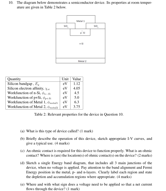
10. The diagram below demonstrates a semiconductor device. Its properties at room temper ature are given in Table 2 belovw Metal 1 Sio Si0 p -Si n-5 Metal 2 Quantity Silicon bandgap, Eg Silicon electron affinity, Xi workfunction of n-Si, фп-Si Workfunction of p+Si, Op+ SteV5.0 Workfunction of Metal 1, @wetan | eV | 6.3 Workfunction of Metal 2, φ,neta!2 | eV | 3.75 Unit Value eV 1.12 eV 4.05 eV 4.5 Table 2: Relevant properties for the device in Question 10 (a) What is this type of device called? (1 mark) (b) Briefly describe the operation of this device, sketch appropriate I-V curves, and give a typical use. (4 marks) (c) An ohmic contact is required for this device to function properly. What is an ohmic contact? Where is (are) the location(s) of ohmic contact s) on the device? (2 marks) (d) Sketch a single Energy band diagram, that includes all 3 main junctions of the device, when no voltage is applied. Pay attention to the band alignment and Fermi Energy position in the metal, p- and n-layers. Clearly label each region and state the depletion and accumulation regions where appropriate. (4 marks) (e) Where and with what sign does a voltage need to be applied so that a net current flows through the device? 1 mark) Show transcribed image text
Expert Answer
Answer to 10 Diagram Demonstrates Semiconductor Device Properties Room Temper Ature Given Table 2 Be Q33025314 . . .
OR