(Solved) : Part1 Part2 Part3 Want Find Part1 Part2 Part3 Waveform Mathematically Want Use Ispice Get Q37803093 . . .
part1.
part.2
part.3
I want to find the part1 part2 part3 waveformmathematically. And I want to use ISPICE to get the part1 part2part3 waveform. please help me!!
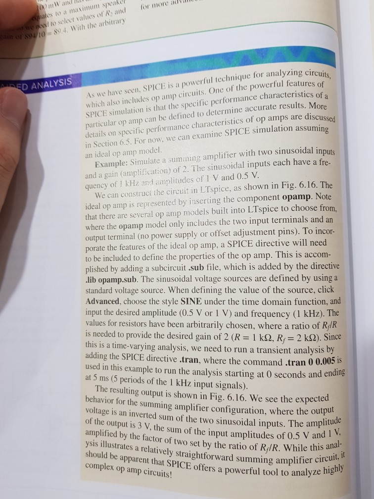
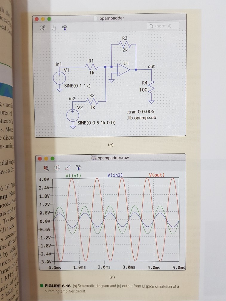
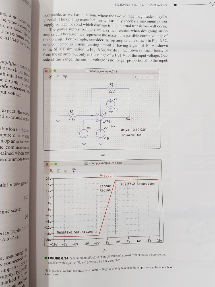
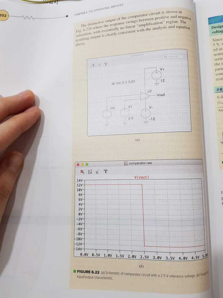
ates to a maximum speake ed to seleet values of & and or more advilll 108o4, With the arbitrary I technique for analyzing circuit One of the powerful features of As we have seen, SPICE is a powerful which also includes op amp circuits. SPICE simulation is that the specific performance characteristics of a particular op amp can be defined to determine accurate results. More details on specific performance cha in Section 6.5. For now, we can ex an ideal op amp model D ANALYSIS racteristics of op amps are discussed amine SPICE simulation assuming Example: Simulate a summing amplifier with two sinusoidal in and a gain (amplification) of 2. The sinusoidal inputs each have a fre- uency of I kHz and amplitudes of 1 V and 0.5 V We can construcí the circuit in LTspice, as shown in Fig. 6.16. The ideal op amp is represented by inserting the component opamp. Note that there are several op amp models built into LTspice to choose from, here the opamp model only includes the two input terminals and an output terminal (no power supply or offset adjustment pins). To incor porate the features of the ideal op amp, a SPICE directive will need to be included to define the properties of the op amp. This is accom plished by adding a subcircuit sub file, which is added by the directive lib opamp.sub. The sinusoidal voltage sources are defined by usinga tandard voltage source. When defining the value of the source, click Advanced, choose the style SINE under the time domain function, and input the desired amplitude (0.5 V or 1 V) and frequency (1 kHz). The values for resistors have been arbitrarily chosen, where a ratio of RylR is needed to provide the desired gain of 2 (R-1 kQ. R.-2 kΩ). Since this is a time-varying analysis, we need to run a transient analysis adding the SPICE directive .tran, where the command .tran 0 0.005 used in this example to run the analysis starting at 0 seconds and ending at 5 ms (5 periods of the 1 kHz input signals) by The resulting output is shown in Fig. 6.16. We see the expecte behavior for the summing amplifier configuration, where the voltage is an inverted sum of the two sinusoidal inputs of the output is 3 V, the sum of the input amplitudes of 0.5 amplified by the factor of two set by the ratio of Rf/R. While ysis illustrates a relatively straightforward summing amplifier c . The amp itu an this a circuit, it should be apparent that SPICE offers a powerful tool to analyze complex op amp circuits! hly opampadder ed Q (normal) R3 2k U1 R1 in 1 out V1 1 k R4 100 SINE (0 1 1k) R2 in2 cir ures of tics of s. Mor discu ssuming V2 1k .tran 0 0.005 .lib opamp.sub SINE(0 0.5 1k 0 0) opampadder.raw idal ip ave a fr V(in1) V(in2) V(out) 3.0V 2.4V 1.8V 1.2V 0.6V 0.0V 6.16. T mp als and 1.2V 1.8V 2.4V j by 3.0v 0.0ms 1.0ms 2.0ms 3.0ms 4.0ms 5.0ms FIGURE 6.16 (d) Schematic diagram and (b) output from LTspice simulation of a summing amplifier circuit. SECTION 6.5 PRACTICAL CONSIDERATIONS us, a non becomes mor n, an ideal a maximum e AD549 hav acceptable, as well as situations where the two voltage magnitudes may be ual. The op amp manufacturer will usually specify a maximum power supply voltage, beyond which damage to the internal transistors will occur The power supply voltages are a critical choice when designing an op amp circuit because they represent the maximum possible output voltage of the op amp. For example, consider the op amp circuit shown in Fig. 6.32 now connected as a noninverting amplifier having a gain of 10. As shown in the SPICE simulation in Fig. 6.34, we do in fact observe linear behavior from the op amp, but only in the range of ±1.71 V for the input voltage. Out- side of this range, the output voltage is no longer proportional to the input, un Op umplifier, since he two input ter th input terminal e op amp is on ode rejection.T put voltage opamp example 741 R2 47k V1 expect the outp d v2 would notbe R1 U1 UA741 V2 (a) 4.7k out ibution to the ou- npare one op amp n op amp to reje e common-mo tained when bot e common-mod dc Vs-10 10 0.01 lib uA741.sub 18 opamp example 741.raw 20V 16V- 12V 8V- 4V- eV- atial-mode gain Positive Saturation Linear Region 12 mic scale: 12 -12V -16V Negative Saturation -28V d in Table 6.3 A to AcM- FIGURE 6.34 Simulated input/output characteristics of a uA741 connected as a noninverting e, assuming mplifier with a gain of 10, and powered by +18 V supplies. ) In practice, we find the maximum output voltage is slighty s connec (3) In practice, we find the maximum output voltage is slightly less than the supply voltage by as much as a volt or so. by as much as amp in or supply, typi marked loedback The Comparator Closed loop is the preferred method of using an op amp as an amplifier, as it serves to isolate the circuit performance from variations in the open-loop n that arise from changes in temperature or manufacturing differences. re are a number of applications, however, where it is advantageous to e an op amp in an open-loop configuration. Devices intended for such lications are often referred to as comparators because they are designed ain 12 V app somewhat in open-loop operation ifferently from regular op amps in order to improve their speed V+ Figure 6.21 shows a simple comparator circuit where a 2.5 V reference ltage is connected to the noninverting input, and the voltage being com red (Vin) is connected to the inverting input. Since the op amp has a very large open-loop gain A, it does not take a large voltage difference between V- 2.5 V 12 V input terminals to drive it into saturation. Thus, a positive 12 V output FIGURE 6.21 An example comparator circult vwith m the comparator indicates that the input voltage is less than the refer- e voltage, and a negative 12 V output indicates an input voltage greater thian the reference (opposite behavior is obtained if we connect the reference a 2.5 V reference voltage enc Itage to the inverting input instead). 12 V, Vin< 2.5 V 12 V, Vin 2.5 V out COMPUTER-AIDED ANALYSIS Let us use SPICE to simulate the comparator circuit shown in Fig. 6.21 While we would still like to use the ideal representation of an op amp, we need to use a SPICE model that defines the power supplies connected to the op amp. In this case, we will use the component UniversalOpAmp2 to describe the op amp, with the resulting schemat- ic shown in Fig. 6.22a. The dependence of vout On Vin can be simulated by using a de sweep command. The SPICE directive .de Vin 0 5 0.01 defines a de sweep of the voltage source Vin starting at 0 V, ending at 5 V, in steps of 0.01V (Continued on next page The distinctive output of the comparator circuit is show Fig, 6.22h where the response swings between positive a saturation, with essentially no linear “amplification” resulting output is above CHAPTER 6 THE OPERATIONAL AMPLIFIER and negati region. The Desigı voltag clearly consistent with the analysis and equatio Since ed as noni serie the i para som testi omparator 12 .dc Vin 0 5 0.01 U2 PR 6.4 V1 Vin V. An 2.5 -12 comparator.raw V(vout) 14V 12V- 0Vt 0V -6V -8V 10V 12V 14V e.ev 0.5V 1.0V 1.5V 2.0v 2.5V 3.0v 3.5V 4.0V 4.3 FIGURE 6.22 (a) Schematic of comparator circuit with a 2.5 V reference voltage. b input’output characteristic. Show transcribed image text
Expert Answer
Answer to Part1 Part2 Part3 Want Find Part1 Part2 Part3 Waveform Mathematically Want Use Ispice Get Q37803093 . . .
OR